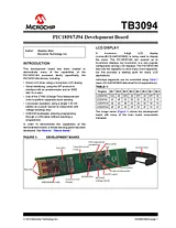
Data SheetTable of ContentsTB30941Introduction1LCD Display1TABLE 1:1FIGURE 1: Development Board1IEEE 802.15.4 Radio2Accelerometer (Motion Sensing)2USB HID BootLoader2FIGURE 2: USB Bootloader Window2Programming/Debug Interface2Power3FIGURE 3: 1.5V battery and MCP1640 boost circuit3Dance Game3Dance Leader3Dance Follower3Baton Operation3FIGURE 4: Front View Baton with X, Y, Z Axes Indicated3Orientation of X, Y, Z Axes3FIGURE 5: Side View of Multiple Dance Batons with X, Y, Z Axes Indicated4Start of Game Play4Accelerometer Sampling4Score Calculation4FIGURE 6: Example of How Score is Released4FIGURE 7: ACCELERATION DATA5Game Winner5Battery Low Indicator5Board Features51. USB HID bootloader – the PIC18F67J94 microcontroller can be reprogrammed using a USB cable.52. Multiple test points:5a) TP1 – DI signal connects to MRF24J40 and RA15b) TP2 – SCK signal connects to accelerometer and RA65c) TP3 – DO signal connects to MRF24J40 and RA05d) TP4 – SDI signal connects to accelerometer and RA45e) TP5 – CLK signal connects to MRF24J40 and RA35f) TP6 – SDO signal connects to accelerometer and RA55g) TP7 – connects to RF5, and commonly used for UART ‘printf’ data5h) TP8 – connects to RF6, and can be user-defined5i) TP9 – CS signal connects to accelerometer and RC75j) TP10 – battery output voltage, connects to RG45k) TP11 – Ground53. ICSP™ programming connection is available on J2. The connector is not populated, but can be added to allow programming with supported Microchip programmers.54. Error messages – Error messages (sent to LCD display) are provided to alert when unintended operation occurs. Unused error messages are available for development use.6TABLE 2:65. Multiple LEDs – LEDs are available to indicate status.6Test Point Flexibility6Appendix A: PIC18F67J94 Development Board Schematic7TABLE 3: Bill of Materials8Trademarks9Worldwide Sales10Size: 683 KBPages: 10Language: EnglishOpen manual
Data SheetTable of ContentsExtreme Low-Power Features:1Universal Serial Bus Features:1Peripheral Features:1Analog Features:1High-Performance CPU:2Special Microcontroller Features:2Pin Diagrams3Table of Contents6Most Current Data Sheet7Errata7Customer Notification System71.0 Device Overview9TABLE 1-1: Device Features for the 64-pin Devices12TABLE 1-2: Device Features for the 80-Pin Devices12TABLE 1-3: DEVICE FEATURES FOR THE 100-PIN DEVICES13FIGURE 1-1: 64-PIN Device Block Diagram14FIGURE 1-2: 80-Pin Device Block Diagram15FIGURE 1-3: 100-PIN Device BLOCK DIAGRAM16TABLE 1-4: PIC18F97J94 PINOUT I/o Descriptions172.0 Guidelines for Getting Started with PIC18FJ Microcontrollers31FIGURE 2-1: Recommended Minimum connections31FIGURE 2-2: Example of MCLR Pin Connections32FIGURE 2-3: Frequency vs. ESR Performance for Suggested Vcap33TABLE 2-1: Suitable Capacitor Equivalents33FIGURE 2-4: DC Bias Voltage vs. Capacitance Characteristics34FIGURE 2-5: Suggested Placement of the Oscillator Circuit353.0 Oscillator Configurations37FIGURE 3-1: PIC18F General System Clock Diagram37FIGURE 3-2: Clock or Instruction Cycle Timing38TABLE 3-1: Configuration Bit Values for Clock Selection39Register 3-1: OSCCON: Oscillator Control Register41Register 3-2: OSCCON2: Oscillator Control Register 242Register 3-3: OSCCON3: Oscillator Control Register 343Register 3-4: OSCCON4: Oscillator Control Register 443Register 3-5: OSCTUNE: FRC Oscillator Tuning Register44Register 3-6: REFOxCON: REFERENCE Clock Output CONTROL REGISTER46Register 3-7: REFOxCON1: REFERENCE Clock Output CONTROL REGISTER 147Register 3-8: REFOxCON2: REFERENCE Clock Output CONTROL REGISTER 248Register 3-9: REFOxCON3: REFERENCE Clock Output CONTROL REGISTER 348TABLE 3-2: Primary Oscillator Operating Modes49FIGURE 3-3: Crystal or Ceramic Resonator Operation (MS or HS Oscillator Mode)49FIGURE 3-4: Example Oscillator/Resonator Start-up Characteristics50FIGURE 3-5: External Clock Input Operation (CLKOEN = 1)52FIGURE 3-6: External Clock Input Operation (CLKOEN = 0)52FIGURE 3-7: Basic Oscillator Block Diagram53FIGURE 3-8: 96 MHz PLL Block54TABLE 3-3: System Clock Options During USB Operation55TABLE 3-4: Valid Primary Oscillator Configurations for USB Operations55FIGURE 3-9: Clock Transition Timing Diagram58FIGURE 3-10: Active Clock Tuning Block Diagram60Register 3-10: ACTCON: Active Clock Tuning (ACT) Control Register614.0 Power-Managed Modes65TABLE 4-1: Summary of Operating Modes for PIC18F97J94 Family Devices with Vbat Power-Saving Features66TABLE 4-2: Bit Settings for All Sleep Modes69TABLE 4-3: Delay Times for Exiting from Sleep Mode70TABLE 4-4: Delay Times for Exiting from Retention Sleep Mode70TABLE 4-5: Bit Settings for All Deep Sleep Modes73TABLE 4-6: Delay Times for Exiting from Deep Sleep Mode73TABLE 4-7: Delay Times for Exiting Retention Deep Sleep Mode74FIGURE 4-1: Vbat Power Topology75Register 4-1: DSCONL: Deep Sleep Control Register Low77Register 4-2: DSCONH: Deep Sleep Control Register HIGH77Register 4-3: DSWAKEL: Deep Sleep Wake-up Source Register Low(1)78Register 4-4: DSWAKEH: Deep Sleep Wake-up Source Register HIgh78Register 4-5: PMD0: Peripheral Module Disable Register 080Register 4-6: PMD1: Peripheral Module Disable Register 181Register 4-7: PMD2: Peripheral Module Disable Register 282Register 4-8: PMD3: Peripheral Module Disable Register 383Register 4-9: PMD4: Peripheral Module Disable Register 4845.0 Reset85FIGURE 5-1: Simplified Block Diagram of On-Chip Reset Circuit85Register 5-1: RCON: Reset Control Register86Register 5-2: RCON2: Reset Control Register 287Register 5-3: RCON3: Reset Control Register 388Register 5-4: RCON4: Reset Control Register 489FIGURE 5-2: POR Module Timing Sequence for Rising Vdd91FIGURE 5-3: External Power-on Reset Circuit (for Slow Vdd Power-up)92TABLE 5-1: BOR Feature Summary(1)93TABLE 5-2: RCONx BIT operation on various Resets and Wake-ups96TABLE 5-3: Initialization Conditions for All Registers976.0 Memory Organization113FIGURE 6-1: Memory Maps for PIC18F97J94 Family Devices113TABLE 6-1: Flash Configuration Word for PIC18F97J94 Family Devices114FIGURE 6-2: Hard Vector for PIC18F97J94 Family Devices114FIGURE 6-3: Return Address Stack and Associated Registers115Register 6-1: STKPTR: Stack Pointer Register116FIGURE 6-4: Clock/ Instruction Cycle118FIGURE 6-5: Instructions in Program Memory119FIGURE 6-6: Data Memory Map for PIC18F97J94 Family Devices121FIGURE 6-7: Use of the Bank Select Register (Direct Addressing)122TABLE 6-2: Register File Summary124Register 6-2: Status Register135FIGURE 6-8: Indirect Addressing137FIGURE 6-9: Comparing Addressing Options for Bit-Oriented and Byte-Oriented Instructions (Extended Instruction Set Enabled)140FIGURE 6-10: Remapping the Access Bank with Indexed Literal Offset Addressing1417.0 Flash Program Memory143FIGURE 7-1: Table Read Operation143FIGURE 7-2: Table Write Operation144Register 7-1: EECON1: EEPROM CONTROL REGISTER 1 (ACCESS FA6h)145TABLE 7-1: Table Pointer Operations with TBLRD and TBLWT Instructions146FIGURE 7-3: Table Pointer Boundaries Based on Operation146FIGURE 7-4: Reads From Flash Program Memory147FIGURE 7-5: Table Writes to Flash Program Memory1498.0 External Memory Bus153TABLE 8-1: PIC18F97J94 Family External Bus – I/O Port Functions153Register 8-1: MEMCON: External Memory Bus Control Register(1)154TABLE 8-2: Address and Data Lines for Different Address and Data Widths155FIGURE 8-1: 16-bit Byte Write Mode Example157FIGURE 8-2: 16-bit Word Write Mode Example158FIGURE 8-3: 16-bit Byte Select Mode Example159FIGURE 8-4: External Memory Bus Timing for TBLRD (Extended Microcontroller Mode)160FIGURE 8-5: External Memory Bus Timing for Sleep (Extended Microcontroller Mode)160FIGURE 8-6: 8-bit Multiplexed Mode Example161FIGURE 8-7: External Memory Bus Timing For TBLRD (Extended Microcontroller Mode)162FIGURE 8-8: External Memory Bus Timing for SLEEP (Extended Microcontroller Mode)162TABLE 8-3: Registers Associated with the External Memory Bus1639.0 8 X 8 Hardware Multiplier165TABLE 9-1: Performance Comparison for Various Multiply Operations16510.0 Interrupts167FIGURE 10-1: PIC18F97J94 Family Interrupt Logic169Register 10-1: INTCON: Interrupt Control Register170Register 10-2: INTCON2: Interrupt Control Register 2171Register 10-3: INTCON3: Interrupt Control Register 3172Register 10-4: PIR1: Peripheral Interrupt Request (Flag) Register 1173Register 10-5: PIR2: Peripheral Interrupt Request (Flag) Register 2174Register 10-6: PIR3: Peripheral Interrupt Request (Flag) Register 3175Register 10-7: PIR4: Peripheral Interrupt Request (Flag) Register 4176Register 10-8: PIR5: Peripheral Interrupt Request (Flag) Register 5178Register 10-9: PIR6: Peripheral Interrupt Request (Flag) Register 6179Register 10-10: PIE1: Peripheral Interrupt Enable Register 1180Register 10-11: PIE2: Peripheral Interrupt Enable Register 2181Register 10-12: PIE3: Peripheral Interrupt Enable Register 3182Register 10-13: PIE4: Peripheral Interrupt Enable Register 4183Register 10-14: PIE5: Peripheral Interrupt Enable Register 5184Register 10-15: PIE6: Peripheral Interrupt Enable Register 6185Register 10-16: IPR1: Peripheral Interrupt Priority Register 1186Register 10-17: IPR2: Peripheral Interrupt Priority Register 2187Register 10-18: IPR3: Peripheral Interrupt Priority Register 3188Register 10-19: IPR4: Peripheral Interrupt Priority Register 4189Register 10-20: IPR5: Peripheral Interrupt Priority Register 5190Register 10-21: IPR6: Peripheral Interrupt Priority Register 6191Register 10-22: RCON: Reset Control Register192Register 10-23: IOCP: Interrupt-On-Change Positive Edge Register194Register 10-24: IOCN: Interrupt-On-Change Negative Edge Register194Register 10-25: IOCF: Interrupt-On-Change Flag Register19411.0 I/O Ports197FIGURE 11-1: Generic I/O Port Operation197Register 11-1: PADCFG1: Pad Configuration Register 1(1)198FIGURE 11-2: Using the Open-Drain Output (USART Shown as Example)199Register 11-2: ODCON1: Peripheral Open-Drain Control Register 1199Register 11-3: ODCON2: Peripheral Open-Drain Control Register 2200TABLE 11-1: PORTA FUNCTIONS201TABLE 11-2: PORTB FUNCTIONS203TABLE 11-3: PORTC Functions205TABLE 11-4: PORTD Functions207TABLE 11-5: PORTE Functions209TABLE 11-6: PORTF Functions211TABLE 11-7: PORTG Functions213TABLE 11-8: PORTH Functions215TABLE 11-9: PORTJ Functions217TABLE 11-10: PORTK Functions219TABLE 11-11: PORTL Functions220FIGURE 11-3: PORTD and PORTE Block Diagram (Parallel Slave Port)221Register 11-4: PSPCON: Parallel Slave Port Control Register222FIGURE 11-4: Parallel Slave Port Write Waveforms222FIGURE 11-5: Parallel Slave Port Read Waveforms223FIGURE 11-6: Structure of Port Shared with PPS Peripherals225FIGURE 11-7: Remappable Input for U1RX226TABLE 11-12: RPINR Registers227TABLE 11-13: RPIn Registers and Available Functions228FIGURE 11-8: MULTIPLEXING OF REMAPPABLE OUTPUT FOR RPn230Register 11-5: RPORn_n: REMAPPED PERIPHERAL OUTPUT REGISTER n (FUNCTION MAPS TO PIN)230TABLE 11-14: PPS-Lite Output23112.0 Data Signal Modulator235FIGURE 12-1: Simplified Block Diagram of the Data SIgnal Modulator236FIGURE 12-2: On-OFF Keying (OOK) Synchronization238FIGURE 12-3: No SYNCHRONIZATION (MDCHSYNC = 0, MDCLSYNC = 0)238FIGURE 12-4: Carrier High SYNCHRONIZATION (MDCHSYNC = 1, MDCLSYNC = 0)238FIGURE 12-5: Carrier Low SYNCHRONIZATION (MDCHSYNC = 0, MDCLSYNC = 1)239FIGURE 12-6: Full Synchronization (MDCHSYNC = 1, MDCLSYNC = 1)239Register 12-1: MDCON: Modulation Control Register241Register 12-2: MDSRC: Modulation Source Control Register242Register 12-3: MDCARH: Modulation Carrier High Control Register243Register 12-4: MDCARL: Modulation Carrier Low Control Register24413.0 Liquid Crystal Display (LCD) Controller245FIGURE 13-1: LCD Controller Module Block Diagram245Register 13-1: LCDCON: LCD Control Register246Register 13-2: LCDREG: LCD Charge Pump Control Register247Register 13-3: LCDPS: LCD Phase Register248TABLE 13-1: LCDSEx REGISTERS AND ASSOCIATED SEGMENTS249Register 13-4: LCDSEx: LCD SEGMENT x Enable Register249Register 13-5: LCDDATAx: LCD DATA x Register250TABLE 13-2: LCDDATA Registers And Bits For Segment And COM Combinations250FIGURE 13-2: LCD Clock Generation251TABLE 13-3: Internal Resistance Ladder Power Modes252FIGURE 13-3: LCD Bias Internal Resistor Ladder Connection Diagram253FIGURE 13-4: LCD Reference Ladder Power Mode Switching Diagram254FIGURE 13-5: Internal Reference And Contrast Control Block Diagram255Register 13-6: LCDREF: LCD Reference Ladder Control Register256Register 13-7: LCDRL: LCD Reference Ladder Control Register Low257Register 13-8: LCDREG: LCD Voltage Regulator Control Register258FIGURE 13-6: LCD Regulator Connections For M0 And M1 Configurations260FIGURE 13-7: Resistor Ladder Connections For M2 Configuration261FIGURE 13-8: Resistor Ladder Connections For M3 Configuration262TABLE 13-4: COM<7:0> Pin Functions264TABLE 13-5: Frame Frequency Formulas264FIGURE 13-9: Type-A/Type-B Waveforms In Static Drive265FIGURE 13-10: Type-A Waveforms In 1/2 Mux, 1/2 Bias Drive266FIGURE 13-11: Type-B Waveforms In 1/2 Mux, 1/2 Bias Drive267FIGURE 13-12: Type-A Waveforms In 1/2 Mux, 1/3 Bias Drive268FIGURE 13-13: Type-B Waveforms In 1/2 Mux, 1/3 Bias Drive269FIGURE 13-14: Type-A Waveforms In 1/3 Mux, 1/2 Bias Drive270FIGURE 13-15: Type-B Waveforms In 1/3 Mux, 1/2 Bias Drive271FIGURE 13-16: Type-A Waveforms In 1/3 Mux, 1/3 Bias Drive272FIGURE 13-17: Type-B Waveforms In 1/3 Mux, 1/3 Bias Drive273FIGURE 13-18: Type-A Waveforms In 1/4 Mux, 1/3 Bias Drive274FIGURE 13-19: Type-B Waveforms In 1/4 Mux, 1/3 Bias Drive275FIGURE 13-20: Type-A Waveforms In 1/8 Mux, 1/3 Bias Drive276FIGURE 13-21: Type-B Waveforms In 1/8 Mux, 1/3 Bias Drive277FIGURE 13-22: Example Waveforms And Interrupt Timing In Quarter Duty Cycle Drive278FIGURE 13-23: Sleep Entry/Exit When SLPEN = 1 or CS<1:0> = 00.28014.0 Timer0 Module281Register 14-1: T0CON: Timer0 Control Register281FIGURE 14-1: Timer0 Block Diagram (8-bit Mode)282FIGURE 14-2: Timer0 Block Diagram (16-bit Mode)28215.0 Timer1/3/5 Modules284Register 15-1: TxCON: Timerx Control Register285Register 15-2: TxGCON: Timerx Gate Control Register(1)286Figure 15-1: TIMER1/3/5 Block Diagram287TABLE 15-1: TIMER1/3/5 GATE ENABLE SELECTIONS289FIGURE 15-2: Timer1/3/5 Gate Count Enable Mode289TABLE 15-2: TIMER1/3/5 GATE SOURCES290FIGURE 15-3: Timer1/3/5 Gate Toggle Mode290FIGURE 15-4: Timer1/3/5 Gate Single Pulse Mode291FIGURE 15-5: Timer1/3/5 Gate Single Pulse and Toggle Combined Mode292TABLE 15-3: Timer1/3/5 Interrupt Flag Bits293TABLE 15-4: Timer1/3/5 Interrupt Enable Bits29316.0 Timer2/4/6/8 Modules294TABLE 16-1: Timer2/4/6/8 Flag Bits294TABLE 16-2: Timer2/4/6/8 Interrupt Enable Bits294Register 16-1: TxCON: Timerx Control Register (Timer2/4/6/8)295FIGURE 16-1: Timer2/4/6/8 Block Diagram29517.0 Real-Time Clock and Calendar (RTCC)297FIGURE 17-1: RTCC Block Diagram297RTCC Control Registers298RTCC Value Registers298Alarm Value Registers298Register 17-1: RTCCON1: RTCC Configuration Register 1(1)299Register 17-2: RTCCAL: RTCC Calibration Register300Register 17-3: RTCCON2: RTC CONFIGURATION REGISTER 2(1)301Register 17-4: ALRMCFG: Alarm Configuration Register302Register 17-5: ALRMRPT: Alarm Repeat Register303Register 17-6: Reserved Register (RTCVALH when RTCPTR<1:0> = 11)303Register 17-7: Year: Year Value Register(1) (RTCVALL when RTCPTR<1:0> = 11)304Register 17-8: MontH: Month Value Register(1) (RTCVALH when RTCPTR<1:0> = 10)304Register 17-9: Day: Day Value Register(1) (RTCVALL when RTCPTR<1:0> = 10)305Register 17-10: Weekday: Weekday Value Register(1) (RTCVALH when RTCPTR<1:0> = 01)305Register 17-11: Hour: Hour Value Register(1) (RTCVALL when RTCPTR<1:0> = 01)305Register 17-12: MINUTE: Minute Value Register (RTCVALH when RTCPTR<1:0> = 00)306Register 17-13: SECOND: Second Value Register (RTCVALL when RTCPTR<1:0> = 00)306Register 17-14: ALRMMNTH: Alarm Month Value Register(1) (ALRMVALH when ALRMPTR<1:0> = 10)307Register 17-15: ALRMDAY: Alarm Day Value Register(1) (ALRMVALL when ALRMPTR<1:0> = 10)307Register 17-16: ALRMWd: Alarm Weekday Value Register(1) (ALRMVALH when ALRMPTR<1:0> = 01)308Register 17-17: ALRMHr: Alarm Hours Value Register(1) (ALRMVALL when ALRMPTR<1:0> = 01)308Register 17-18: ALRMMIN: Alarm Minutes Value Register (ALRMVALH when ALRMPTR<1:0> = 00)309Register 17-19: ALRMSEC: Alarm Seconds Value Register (ALRMVALL when ALRMPTR<1:0> = 00)309FIGURE 17-2: Timer Digit Format310FIGURE 17-3: Alarm Digit Format310FIGURE 17-4: Clock Source Multiplexing311TABLE 17-1: Day of Week Schedule311TABLE 17-2: Day to Month Rollover Schedule311TABLE 17-3: RTCVALH and RTCVALL Register Mapping312TABLE 17-4: ALRMVAL Register Mapping313FIGURE 17-5: Alarm Mask Settings314FIGURE 17-6: Timer Pulse Generation315TABLE 17-5: RTCC Control Registers316TABLE 17-6: RTCC Value Registers316TABLE 17-7: Alarm Value Registers31618.0 Enhanced Capture/Compare/PWM (ECCP) Module317Register 18-1: CCPxCON: Enhanced Capture/Compare/PWM x Control318Register 18-2: CCPTMRS0: CCP Timer Select 0 Register319TABLE 18-1: ECCP Mode – Timer Resource320TABLE 18-2: ECCP1/2/3 Interrupt Flag Bits321FIGURE 18-1: Capture Mode Operation Block Diagram321FIGURE 18-2: Compare Mode Operation Block Diagram322FIGURE 18-3: Example Simplified Block Diagram of the Enhanced PWM Mode323TABLE 18-3: Example Pin Assignments for Various PWM Enhanced Modes324FIGURE 18-4: Example PWM (enhanced Mode) Output Relationships (Active-High State)324FIGURE 18-5: Example Enhanced PWM Output Relationships (Active-Low State)325FIGURE 18-6: Example of Half-Bridge PWM Output326FIGURE 18-7: Example of Half-Bridge Applications326FIGURE 18-8: Example of Full-Bridge Application327FIGURE 18-9: Example of Full-Bridge PWM Output328FIGURE 18-10: Example of PWM Direction Change329FIGURE 18-11: Example of PWM Direction Change at Near 100% Duty Cycle330Register 18-3: ECCPxAS: ECCPx Auto-Shutdown Control Register(1,2,3)331FIGURE 18-12: PWM Auto-shutdown With Firmware Restart (PxRSEN = 0)332FIGURE 18-13: PWM Auto-shutdown With Auto-Restart Enabled (PxRSEN = 1)332FIGURE 18-14: Example of Half-Bridge PWM Output333FIGURE 18-15: Example of Half-Bridge Applications333Register 18-4: ECCPxDEL: Enhanced PWM CONTROL REGISTER x334Register 18-5: PSTRxCON: Pulse Steering Control(1)335FIGURE 18-16: Simplified Steering Block Diagram336FIGURE 18-17: Example of Steering Event at End of Instruction (STRSYNC = 0)336FIGURE 18-18: Example of Steering Event at Beginning of Instruction (STRSYNC = 1)33619.0 Capture/Compare/PWM (CCP) Modules339Register 19-1: CCPxCON: CCPx Control Register (CCP4-CCP10 Modules)339Register 19-2: CCPTMRS1: CCP Timer Select Register 1340Register 19-3: CCPTMRS2: CCP Timer Select Register 2341Register 19-4: CCPRxL: CCPx Period Low Byte Register342Register 19-5: CCPRxH: CCPx Period High Byte Register342TABLE 19-1: CCP Mode – Timer Resource343TABLE 19-2: Timer Assignments for CCP Modules 4, 5, 6 and 7343TABLE 19-3: Timer Assignments for CCP Modules 8, 9 and 10343FIGURE 19-1: Capture Mode Operation Block Diagram345FIGURE 19-2: Compare Mode Operation Block Diagram347FIGURE 19-3: Simplified PWM Block Diagram348FIGURE 19-4: PWM Output348TABLE 19-4: Example PWM Frequencies and Resolutions at 40 MHz34920.0 Master Synchronous Serial Port (MSSP) Module351FIGURE 20-1: MSSPx Block Diagram (SPI Mode)352Register 20-1: SSPxSTAT: MSSPx STATUS REGISTER (SPI MODE)353Register 20-2: SSPxCON1: MSSPx CONTROL REGISTER 1 (SPI MODE)354Register 20-3: SSPxCON3: MSSP CONTROL REGISTER 3 (SPI MODE)355FIGURE 20-2: SPI Master/Slave Connection357FIGURE 20-3: SPI Mode Waveform (Master Mode)358FIGURE 20-4: Slave Synchronization Waveform359FIGURE 20-5: SPI Mode Waveform (Slave Mode with CKE = 0)360FIGURE 20-6: SPI Mode Waveform (Slave Mode with CKE = 1)360TABLE 20-1: SPI Bus Modes361Register 20-4: DMACON1: DMA CONTROL REGISTER 1364Register 20-5: DMACON2: DMA CONTROL REGISTER 2365FIGURE 20-7: MSSPx Block Diagram (I2C™ Mode)372Register 20-6: SSPxSTAT: MSSPx STATUS REGISTER (I2C™ MODE)373Register 20-7: SSPxCON1: MSSPx CONTROL REGISTER 1 (I2C™ MODE)374Register 20-8: SSPxCON2: MSSPx Control Register 2 (I2C™ Master Mode)375Register 20-9: SSPxCON3: MSSP CONTROL REGISTER 3 (I2C Master MODE)376Register 20-10: SSPxCON2: MSSPx Control Register 2 (I2C™ Slave Mode)377Register 20-11: SSPxCON3: MSSP CONTROL REGISTER 3 (I2C Slave MODE)378Register 20-12: SSPxMSK: MSSPx I2C™ Slave Address Mask Register (7-bit Masking Mode)(1)379FIGURE 20-8: I2C™ Slave Mode Timing with SEN = 0 (Reception, 7-bit Address)384FIGURE 20-9: I2C™ Slave Mode Timing with SEN = 0 and MSK<5:1> = 01011 (Reception, 7-bit Address)385FIGURE 20-10: I2C™ Slave Mode Timing (Transmission, 7-bit Address)386FIGURE 20-11: I2C™ Slave Mode Timing with SEN = 0 and MSK<5:1> = 01001 (Reception, 10-bit Address)387FIGURE 20-12: I2C™ Slave Mode Timing with SEN = 0 (Reception, 10-bit Address)388FIGURE 20-13: I2C™ Slave Mode Timing (Transmission, 10-bit Address)389FIGURE 20-14: Clock Synchronization Timing391FIGURE 20-15: I2C™ Slave Mode Timing with SEN = 1 (Reception, 7-bit Address)392FIGURE 20-16: I2C™ Slave Mode Timing with SEN = 1 (Reception, 10-bit Address)393FIGURE 20-17: Slave Mode General Call Address Sequence (7 or 10-bit Addressing Mode)394FIGURE 20-18: MSSPx Block Diagram (I2C™ Master Mode)395FIGURE 20-19: Baud Rate Generator Block Diagram397TABLE 20-2: I2C™ Clock Rate w/BRG397FIGURE 20-20: Baud Rate Generator Timing with Clock Arbitration398FIGURE 20-21: First Start Bit Timing399FIGURE 20-22: Repeated Start Condition Waveform400FIGURE 20-23: I2C™ Master Mode Waveform (Transmission, 7 or 10-bit Address)402FIGURE 20-24: I2C™ Master Mode Waveform (Reception, 7-bit Address)403FIGURE 20-25: Acknowledge Sequence Waveform404FIGURE 20-26: Stop Condition Receive or Transmit Mode404FIGURE 20-27: Bus Collision Timing for Transmit and Acknowledge405FIGURE 20-28: Bus Collision During Start Condition (SDAx Only)406FIGURE 20-29: Bus Collision During Start Condition (SCLx = 0)407FIGURE 20-30: BRG Reset Due to SDAx Arbitration During Start Condition407FIGURE 20-31: Bus Collision During a Repeated Start Condition (Case 1)408FIGURE 20-32: Bus Collision During Repeated Start Condition (Case 2)408FIGURE 20-33: Bus Collision During a Stop Condition (Case 1)409FIGURE 20-34: Bus Collision During a Stop Condition (Case 2)40921.0 Enhanced Universal Synchronous Asynchronous Receiver Transmitter (EUSART)411Register 21-1: TXSTAx: EUSARTx Transmit Status And Control Register412Register 21-2: RCSTAx: EUSARTx Receive Status And Control Register413Register 21-3: BAUDCONx: Baud Rate Control Register x414TABLE 21-1: Baud Rate Formulas416TABLE 21-2: Baud Rates for Asynchronous Modes417TABLE 21-3: BRG Counter Clock Rates419FIGURE 21-1: Automatic Baud Rate Calculation420FIGURE 21-2: BRG Overflow Sequence420FIGURE 21-3: EUSARTx Transmit Block Diagram421FIGURE 21-4: Asynchronous Transmission422FIGURE 21-5: Asynchronous Transmission (Back-to-Back)422FIGURE 21-6: EUSARTx Receive Block Diagram423FIGURE 21-7: Asynchronous Reception424FIGURE 21-8: Auto-Wake-up Bit (WUE) Timings During Normal Operation425FIGURE 21-9: Auto-Wake-up Bit (WUE) Timings During Sleep425FIGURE 21-10: Send Break Character Sequence426FIGURE 21-11: Synchronous Transmission428FIGURE 21-12: Synchronous Transmission (Through TXEN)428FIGURE 21-13: Synchronous Reception (Master Mode, SREN)429FIGURE 21-14: BCLK OUTPUT vs. BRG Programming431FIGURE 21-15: IrDA® Encoding Scheme432FIGURE 21-16: Inverted IrDA® Encoding (TXCKP = 1)432FIGURE 21-17: ‘0’ bit Data IrDA® Encoding Scheme432FIGURE 21-18: Macro View of IrDA® Decoding Scheme (RXDTP = 0)433FIGURE 21-19: Inverted Polarity Decoding Results (RXDTP = 1)433FIGURE 21-20: Clock Jitter causing a pulse between consecutive zeros43322.0 12-Bit A/D Converter with Threshold Scan435FIGURE 22-1: 12-Bit A/D Converter Block Diagram (PIC18F97J94 Family)436Register 22-1: ANCON1: ANALOG SELECT CONTROL REGISTER 1 (FOR AN7-AN0)438Register 22-2: ANCON2: ANALOG SELECT CONTROL REGISTER 2 (FOR AN15-AN8)439Register 22-3: ANCON3: ANALOG SELECT CONTROL REGISTER 3 (FOR AN23-AN16)440Register 22-4: AdcoN1H: A/D Control Register 1 High441Register 22-5: ADCON1L: A/D Control Register 1 Low442Register 22-6: ADCON2H: A/D Control Register 2 High443Register 22-7: ADCON2L: A/D Control Register 2 Low444Register 22-8: ADCON3H: A/D Control Register 3 High445Register 22-9: ADCON3L: A/D Control Register 3 Low445Register 22-10: ADCON5H: A/D Control Register 5 High446Register 22-11: ADCON5L: A/D Control Register 5 Low447Register 22-12: ADCHS0H: A/D Sample Select Register 0 High448Register 22-13: ADCHS0L: A/D Sample Select Register 0 Low449Register 22-14: ADHIT1H: A/D Scan Compare Hit Register 1 High (High Word)450Register 22-15: ADHIT1L: A/D Scan Compare Hit Register 1 Low (Low Word)450Register 22-16: ADHIT0H: A/D Scan Compare Hit Register 0 High (High Word)451Register 22-17: ADHIT0L: A/D Scan Compare Hit Register 0 Low (Low Word)451Register 22-18: ADCSS1H: A/D Input Scan Select Register 1 High (High Word)452Register 22-19: ADCSS1L: A/D Input Scan Select Register 1 LOW (Low Word)452Register 22-20: ADCSS0H: A/D Input Scan Select Register 0 High (High word)453Register 22-21: ADCSS0L: A/D Input Scan Select Register 0 Low (Low word)453Register 22-22: ADCTMUEN1H: CTMU Enable Register 1 High (High Word)(1)454Register 22-23: ADCTMUEN1L: CTMU Enable Register 1 Low (Low Word)(1)454Register 22-24: ADCTMUEN0H: CTMU Enable Register 0 High (High Word)(1)455Register 22-25: ADCTMUEN0L: CTMU Enable Register 0 Low (Low Word)(1)455FIGURE 22-2: A/D Sample/Convert Sequence456FIGURE 22-3: A/D Module State Machine Model457TABLE 22-1: A/D Module Functions by Registers and Bits458FIGURE 22-4: CONVERTING ONE CHANNEL, MANUAL SAMPLE START, MANUAL CONVERSION START462FIGURE 22-5: Converting One Channel, Automatic Sample Start, Manual Conversion Start462FIGURE 22-6: Converting One Channel, Manual Sample Start, Tad-Based Conversion Start463FIGURE 22-7: Converting One Channel, Auto-Sample Start, Tad-Based Conversion Start464FIGURE 22-8: Manual Sample Start, Conversion Trigger-Based Conversion Start465FIGURE 22-9: Auto-Sample Start, Conversion Trigger-Based Conversion Start465FIGURE 22-10: A/D Output Data Formats (12-Bit)467TABLE 22-2: Numerical Equivalents of Various Result Codes: 12-Bit Integer Formats468TABLE 22-3: Numerical Equivalents of Various Result Codes: 12-Bit Fractional Formats468FIGURE 22-11: A/D Output Data Formats (10-Bit)468TABLE 22-4: Numerical Equivalents of Various Result Codes: 10-Bit Integer Formats469TABLE 22-5: Numerical Equivalents of Various Result Codes: 10-Bit Fractional Formats469FIGURE 22-12: Simple Comparison Operations (Greater Than and Less Than)472FIGURE 22-13: Inside Window Comparison Operation473FIGURE 22-14: Outside Window Comparison Operation (Over Threshold 2)474FIGURE 22-15: Outside Window Comparison Operation (Under Threshold 1)475FIGURE 22-16: Converting One Channel 16 Times Per Interrupt477FIGURE 22-17: Scanning All 16 Inputs Per Single Interrupt479FIGURE 22-18: Converting a Single Channel, Once Per Interrupt, Using Dual, 8-Word Buffers481FIGURE 22-19: Converting Two Inputs Using Alternating Input Selections483FIGURE 22-20: 12-Bit A/D Converter Analog Input Model485FIGURE 22-21: 12-Bit A/D Transfer Function486FIGURE 22-22: 10-Bit A/D Transfer Function48723.0 Comparator Module489FIGURE 23-1: Comparator Simplified Block Diagram489Register 23-1: CMxCON: Comparator Control x Register490Register 23-2: CMSTAT: Comparator Status Register491FIGURE 23-2: Single Comparator492FIGURE 23-3: Comparator Analog Input Model492TABLE 23-1: Comparator Inputs and Outputs493FIGURE 23-4: Comparator Configurations494TABLE 23-2: Comparator Interrupt Generation49524.0 Comparator Voltage Reference Module497Register 24-1: CVRCONH: Comparator Voltage Reference Control Register High497Register 24-2: CVRCONL: Comparator Voltage Reference Control Register Low498FIGURE 24-1: Comparator Voltage Reference Block Diagram498FIGURE 24-2: Comparator Voltage Reference Output Buffer Example49925.0 High/Low-Voltage Detect (HLVD)501Register 25-1: HLVDCON: High/Low-Voltage Detect Control Register501FIGURE 25-1: HLVD Module Block Diagram (with External Input)502FIGURE 25-2: Low-Voltage Detect Operation (VDIRMAG = 0)504FIGURE 25-3: High-Voltage Detect Operation (VDIRMAG = 1)504FIGURE 25-4: Typical Low-Voltage Detect Application50526.0 Charge Time Measurement Unit (CTMU)507FIGURE 26-1: CTMU Block Diagram507Register 26-1: CTMUCON1: CTMU Control Register 1508Register 26-2: CTMUCON2: CTMU current Control Register 2509Register 26-3: CTMUCON3: CTMU Current Control Register 3510Register 26-4: CTMUCON4: CTMU Current Control Register 4511FIGURE 26-2: CTMU Current Source Calibration Circuit514FIGURE 26-3: CTMU Typical Connections and Internal Configuration for Time Measurement521FIGURE 26-4: CTMU Temperature Measurement Circuit52227.0 Universal Serial Bus (USB)525FIGURE 27-1: USB Peripheral and Options525Register 27-1: UCON: USB CONTROL REGISTER527Register 27-2: UCFG: USB CONFIGURATION REGISTER529FIGURE 27-2: External Circuitry530FIGURE 27-3: USTAT FIFO531Register 27-3: USTAT: USB STATUS REGISTER (ACCESS F64h)531Register 27-4: UEPn: USB ENDPOINT n CONTROL REGISTER (UEP0 THROUGH UEP15)532FIGURE 27-4: Implementation of USB RAM in Data Memory Space533FIGURE 27-5: Example of a Buffer Descriptor534TABLE 27-1: Effect of DTSEN Bit on Odd/Even (DATA0/DATA1) Packet Reception535Register 27-5: BDnSTAT: Buffer Descriptor n Status Register (BD0STAT Through BD63STAT), CPU Mode536Register 27-6: BDnSTAT: Buffer Descriptor n Status Register (BD0STAT Through BD63STAT), SIE Mode (Data Returned By the SIE to the MCU)537FIGURE 27-6: Buffer Descriptor Table Mapping for Buffering Modes538TABLE 27-2: Assignment of Buffer Descriptors for the Different Buffering Modes539TABLE 27-3: Summary of USB Buffer Descriptor Table Registers539FIGURE 27-7: USB Interrupt Logic Funnel540FIGURE 27-8: Example of a USB Transaction and Interrupt Events540Register 27-7: UIR: USB INTERRUPT STATUS REGISTER (ACCESS F62h)541Register 27-8: UIE: USB INTERRUPT ENABLE REGISTER543Register 27-9: UEIR: USB ERROR INTERRUPT STATUS REGISTER (ACCESS F63h)544Register 27-10: UEIE: USB ERROR INTERRUPT ENABLE REGISTER (BANKED F37h)545FIGURE 27-9: Bus Power Only546FIGURE 27-10: Self-power Only546FIGURE 27-11: Dual Power with Self-Power Dominance546TABLE 27-4: Registers Associated with USB Module Operation(1)549FIGURE 27-12: USB Layers55028.0 Special Features of the CPU553TABLE 28-1: MAPPING OF THE FLASH CONFIGURATION WORDS TO THE CONFIGURATION REGISTERS554TABLE 28-2: CONFIGURATION BITS AND DEVICE IDs554Register 28-1: CONFIG1L: Configuration Register 1 lOW (Byte Address 300000h)555Register 28-2: CONFIG1H: Configuration Register 1 High (Byte Address 300001h)555Register 28-3: CONFIG2L: Configuration Register 2 Low (Byte Address 300002h)(1,2,3,4)556Register 28-4: CONFIG2H: Configuration Register 2 High (Byte Address 300003h)(1,2)557Register 28-5: CONFIG3L: Configuration Register 3 Low (Byte Address 300004h)(1,2)558Register 28-6: CONFIG4L: Configuration Register 4 Low (Byte Address 300006h)559Register 28-7: CONFIG4H: Configuration Register 4 High (Byte Address 300007h)559Register 28-8: CONFIG5L: Configuration Register 5 Low (Byte Address 300008h)560Register 28-9: CONFIG5H: Configuration Register 5 High (Byte Address 300009h)561Register 28-10: CONFIG6L: Configuration Register 6 Low (Byte Address 30000Ah)562Register 28-11: CONFIG6H: Configuration Register 6 High (Byte Address 30000Bh)563Register 28-12: CONFIG7L: Configuration Register 7 Low (Byte Address 30000Ch)564Register 28-13: CONFIG8L: Configuration Register 8 Low (Byte Address 30000Eh)565Register 28-14: CONFIG8H: Configuration Register 8 High (Byte Address 30000Fh)566Register 28-15: DEVID2: Device ID Register 2 for the PIC18F97J94567Register 28-16: DEVID1: Device ID Register 1 for the PIC18F97J94567FIGURE 28-1: WDT Block Diagram568Register 28-17: RCON2: Reset Control Register 2569FIGURE 28-2: Timing Transition for Two-Speed Start-up (INTOSC to HSPLL)570FIGURE 28-3: FSCM Block Diagram571FIGURE 28-4: FSCM Timing Diagram572TABLE 28-3: Debugger Resources57329.0 Instruction Set Summary575TABLE 29-1: Opcode Field Descriptions576FIGURE 29-1: General Format for Instructions577TABLE 29-2: PIC18F97J94 Family Instruction Set578TABLE 29-3: Extensions to the PIC18 Instruction Set61730.0 Development Support62531.0 Electrical Characteristics629Absolute Maximum Ratings(†)629FIGURE 31-1: Voltage-frequency Graph, Regulator Disabled (Industrial)(1,2)630TABLE 31-1: DC Characteristics: Power-Down and Supply Current PIC18F97J94 Family (Industrial)632TABLE 31-2: DC Characteristics: Power-Down and Supply Current PIC18F97J94 Family (Industrial)633TABLE 31-3: DC Characteristics: Power-Down and Supply Current PIC18F97J94 Family (Industrial)633TABLE 31-4: DC Characteristics: Power-Down and Supply Current PIC18F97J94 Family (Industrial)634TABLE 31-5: DC Characteristics: Power-Down and Supply Current PIC18F97J94 Family (Industrial)635TABLE 31-6: DC Characteristics: Power-Down and Supply Current PIC18F97J94 Family (Industrial)635TABLE 31-7: DC Characteristics: Power-Down and Supply Current PIC18F97J94 Family (Industrial)636TABLE 31-8: DC Characteristics: CTMU Current Source Specifications637TABLE 31-9: Memory Programming Requirements637TABLE 31-10: Comparator Specifications638TABLE 31-11: Comparator Voltage Reference Specifications638TABLE 31-12: Internal Voltage Regulator Specifications638TABLE 31-13: RC Oscillator Start-Up Time638TABLE 31-14: USB Module Specifications639TABLE 31-15: Temperature and Voltage Specifications – AC641FIGURE 31-2: Load Conditions for Device Timing Specifications641FIGURE 31-3: External Clock Timing642TABLE 31-16: External Clock Timing Requirements642TABLE 31-17: PLL Clock Timing Specifications (Vdd = 2.0V to 3.6V)(1)643TABLE 31-18: Internal RC Accuracy (FRC)643FIGURE 31-4: CLKO and I/O Timing644TABLE 31-19: CLKO and I/O Timing Requirements644FIGURE 31-5: Program Memory Fetch Timing Diagram (8-Bit)645TABLE 31-20: Program Memory Fetch Timing Requirements (8-Bit)645FIGURE 31-6: Program Memory Read Timing Diagram646TABLE 31-21: CLKO and I/O Timing Requirements646FIGURE 31-7: Reset, Watchdog Timer, Oscillator Start-up Timer and Power-up Timer Timing647FIGURE 31-8: Brown-out Reset Timing647TABLE 31-22: Reset, Watchdog Timer, Oscillator Start-up Timer, Power-up Timer and Brown-out Reset Requirements647FIGURE 31-9: High/Low-Voltage Detect Characteristics648TABLE 31-23: High/Low-Voltage Detect Characteristics648FIGURE 31-10: Timer0 and Timer1 External Clock Timings649TABLE 31-24: Timer0 and Timer1 External Clock Requirements649FIGURE 31-11: Capture/Compare/PWM Timings (CCP1, CCP2 Modules)650TABLE 31-25: Capture/Compare/PWM Requirements (CCP1, CCP2 Modules)650FIGURE 31-12: Example SPI Master Mode Timing (CKE = 0)651TABLE 31-26: Example SPI Mode Requirements (Master Mode, Cke = 0)651FIGURE 31-13: Example SPI Master Mode Timing (CKE = 1)652TABLE 31-27: Example SPI Mode Requirements (Master Mode, CKE = 1)652FIGURE 31-14: Example SPI Slave Mode Timing (CKE = 0)653TABLE 31-28: Example SPI Mode Requirements (Slave Mode Timing, CKE = 0)653FIGURE 31-15: Example SPI Slave Mode Timing (CKE = 1)654TABLE 31-29: Example SPI Slave Mode Requirements (CKE = 1)654FIGURE 31-16: I2C™ Bus Start/Stop Bits Timing655TABLE 31-30: I2C™ Bus Start/Stop Bits Requirements (Slave Mode)655FIGURE 31-17: I2C™ Bus Data Timing656TABLE 31-31: I2C™ Bus Data Requirements (Slave Mode)656FIGURE 31-18: MSSPx I2C™ Bus Start/Stop Bits Timing Waveforms657TABLE 31-32: MSSPx I2C™ Bus Start/Stop Bits Requirements657FIGURE 31-19: MSSPx I2C™ Bus Data Timing657TABLE 31-33: MSSPx I2C™ Bus Data Requirements658FIGURE 31-20: EUSARTx Synchronous Transmission (Master/Slave) Timing659TABLE 31-34: EUSARTx/AUSARTx Synchronous Transmission Requirements659FIGURE 31-21: EUSARTx/AUSARTx Synchronous Receive (Master/Slave) Timing659TABLE 31-35: EUSARTx/AUSARTx Synchronous Receive Requirements659TABLE 31-36: A/D Converter Characteristics: PIC18F97J94 (Industrial)660FIGURE 31-22: A/D Conversion Timing661TABLE 31-37: A/D Conversion Requirements66132.0 Packaging Information663Appendix A: Revision History677INDEX679Numerics679A679B679C680D681E681F682G682H682I682L683M684N684O684P684Q685R685S687T687U689V689W689X689The Microchip Web Site691Customer Change Notification Service691Customer Support691Reader Response692Product Identification System693Trademarks695Worldwide Sales696Size: 9.88 MBPages: 696Language: EnglishOpen manual