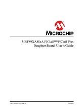
User Manual (MRF89XAM8A-I/RM)Table of ContentsPreface5Chapter 1. Overview91.1 Introduction91.2 MRF89XAMxA PICtail/PICtail Plus Daughter Board Contents9Table 1-1: MRF89XAMxA PICtail™/PICtail Plus Daughter Board91.3 MRF89XAMxA PICtail/PICtail Plus Daughter Board9Figure 1-1: MRF89XAMxA PICtail™/PICtail Plus Daughter Board10Chapter 2. Getting Started112.1 Introduction112.2 Plugging into the PIC18 Explorer Board11Figure 2-1: MRF89XAMxA PICtail™/PICtail Plus Daughter Board plugged into PIC18 Explorer Board122.3 Plugging into the Explorer 16 Development Board12Figure 2-2: MRF89XAMxA PICtail™/PICtail Plus Daughter Board plugged into Explorer 16 Development Board132.4 Downloading and Running the Demo Program13Appendix A. MRF89XAMxA PICtail/PICtail Plus Daughter Board Schematic15A.1 Introduction15A.2 MRF89XAMxA PICtail/PICtail Plus Daughter Board Schematic16Figure A-1: MRF89XAMxA PICtail™/PICtail Plus Daughter Board Schematic16A.3 MRF89XAMxA PICtail/PICtail Plus Daughter Board PCB Layout17Figure A-2: MRF89XAMxA PICtail™/PICtail Plus Daughter Board Top Silkscreen17Figure A-3: MRF89XAMxA PICtail™/PICtail Plus Daughter Board Top Copper17Figure A-4: MRF89XAMxA PICtail™/PICtail Plus Daughter Board Bottom Copper18Figure A-5: MRF89XAMxA PICtail™/PICtail Plus Daughter Board Bottom Silkscreen18A.4 MRF89XAMxA PICtail/PICtail Plus Daughter Board Bill of Materials19Table A-1: MRF89XAMxA PICtail™/PICtail Plus Daughter Board Bill of Materials19Worldwide Sales and Service21Size: 556 KBPages: 21Language: EnglishOpen manual
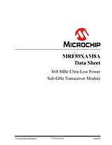
Data Sheet (MRF89XAM8A-I/RM)Table of ContentsFeatures3Operational3RF/Analog Features3Media Access Controller (MAC)/Baseband Features3Media Access Controller (MAC)/Baseband Features3Pin diagram3Table of Contents4Most Current Data Sheet4Errata4Customer Notification System41.0 Device Overview51.1 Interface description5FIGURE 1-1: MRF89XAM8A Block Diagram5TABLE 1-1: Pin description6FIGURE 1-2: Microcontroller to MRF89XAM8A Interface61.2 Mounting Details7FIGURE 1-3: Module details7FIGURE 1-4: Recommended PCB footprint8FIGURE 1-5: Mounting details91.3 Operation101.3.1 Reset101.3.2 Crystal Frequency101.3.3 Clock Output (CLKOUT)101.3.4 Frequency Shift Keying Modulation (FSK)101.3.5 ON-OFF Keying Modulation (OOK)102.0 Circuit Description112.1 Module Schematic11FIGURE 2-1: MRF89XAM8A Application Schematic11FIGURE 2-2: MRF89XAM8A schematic12TABLE 2-1: MRF89XAM8A bill of materials132.2 Printed Circuit Board14FIGURE 2-3: top silk screen14FIGURE 2-4: top copper14FIGURE 2-5: layer 2 — ground plane14FIGURE 2-6: layer 3 — power plane14FIGURE 2-7: bottom copper15FIGURE 2-8: BOttom silk screen15FIGURE 2-9: PCB layer stack up162.3 PCB Antenna16FIGURE 2-10: PCB ANTENNA DIMENSIONS16FIGURE 2-11: pcb antenna simulation drawing17FIGURE 2-12: simulated 2d radiation patteRN17FIGURE 2-13: Simulated 3d radiation patteRN18FIGURE 2-14: simulated PCB antenna impedance18FIGURE 2-15: Simulated PCB Antenna VSWR193.0 Regulatory Approval213.1 Europe213.1.1 Helpful Web Sites21TABLE 3-1: Emissions and Immunity Standards Tested214.0 Electrical Characteristics23Absolute Maximum Ratings23TABLE 4-1: Recommended Operating Conditions24TABLE 4-2: Current Consumption24TABLE 4-3: Digital I/O Pin Input Specifications(1)24TABLE 4-4: PLL Parameters AC Characteristics(1)25TABLE 4-5: Receiver AC Characteristics(1)26TABLE 4-6: Transmitter AC Characteristics(1)274.1 Timing Specification and Diagram28TABLE 4-7: SPI Timing Specification(1,2)28Appendix A: Revision History29Revision A (November 2010)29The Microchip Web Site31Customer Change Notification Service31Customer Support31Reader Response32Product Identification System33Size: 654 KBPages: 34Language: EnglishOpen manual